July 20, 2018
By: Michael Feldman
The upcoming battle between AMD’s “Rome” server CPU and Intel’s “Ice Lake” Xeon scalable processor promises to be an interesting matchup. But this time around, AMD could have an advantage it has never had before.
 Rome, which will be based on AMD’s second-generation Zen architecture (Zen 2), is scheduled to start sampling in the second half of 2018, with full production in 2019. It will be manufactured by either TSMC or GlobalFoundries, or perhaps both, using their respective 7nm process technologies. According to the latest rumors, the chip will deliver a 10 to 15 percent improvement in instructions per clock (IPC) compared to the first-generation EPYC processor and will be equipped with up to 64 cores. That’s a doubling of the core count of the EPYC CPUs, which are being manufactured by GlobalFoundries on its 14nm process.
Very little is known about Ice Lake, Intel’s next-generation Xeon microarchitecture that will purportedly be built on the company’s 10nm semiconductor process. The Power Stamp Alliance has provided a few details revealing the product will include up to eight memory channels and draw as much as 230 watts of power. That suggests a higher count than the current “Skylake” Xeon-SP processors, which top out at 28 cores. It could also mean special IP blocks – graphics processing, extra-wide vector units, integrated FPGAs, etc. – will be offered as part of the package.
What is better known is that Intel’s 10nm technology has suffered multiple delays and is currently not expected to be ready for mass production until sometime in 2019. Originally, the chipmaker was planning to deliver its “Cascade Lake” Xeons on 10nm as a process shrink of “Skylake,” but the delays forced them was to move this product to their latest 14nm node (14nm++). The Cascade Lake Xeon-SP is slated for release later this year.
As a consequence, Ice Lake’s debut on 10nm will be one of those rare instances where Intel will advance the microarchitecture and process node of a Xeon product in tandem. The state of affairs was summed up by Intel CEO (and now ex-CEO) Brian Krzanich, during the first quarter earnings report back in April:
“We continue to make progress on our 10-nanometer process. We are shipping in low volume and yields are improving, though the rate of improvement is slower than we anticipated. As a result, volume production is moving from the second half of 2018 into 2019. We understand the yield issues and have defined improvements for them, but they will take time to implement and qualify. We have leadership products on the roadmap that continue to take advantage of 14-nanometer, with Whiskey Lake for clients and Cascade Lake for the data center coming later this year.”
Anyone who has been following the semiconductor tech space knows that transistor feature sizes advertised by different manufacturers are not comparable. In other words, a 10nm Intel process is not the same size as a 10nm process from TSMC. That’s mostly because there are different ways to measure transistors geometries in the era of 3D FinFET technology. In general, Intel is more conservative with its measurements, such that its nodes correspond to smaller nodes from Samsung, TSMC, and GlobalFoundries.
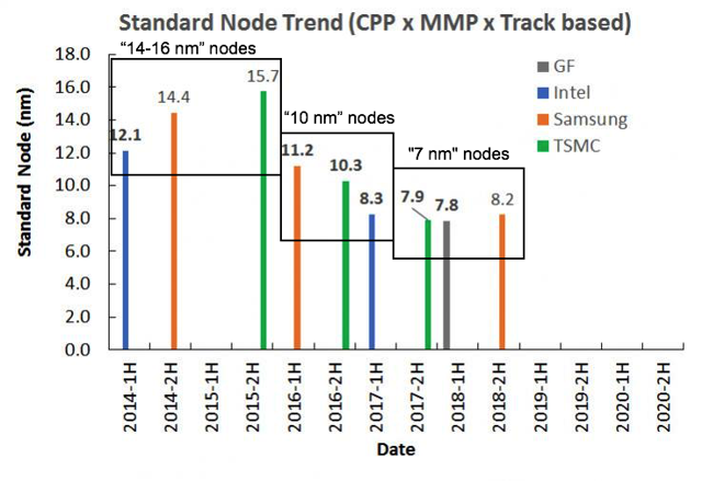
So how will Intel’s 10nm technology match up against the 7nm process nodes from TSMC and GlobalFoundries? If you can believe Scotten Jones’ analysis at SemiWiki.com, the three are pretty much on par, although the 7nm nodes from both TSMC and GlobalFoundries have a slight edge when compared Intel’s 10nm node. Jones uses a “standard node” designation that normalizes feature sizes across manufacturers based on transistor density. His overall conclusion is that “Intel has lost their multiyear density lead over the foundries.” In a writeup by Mark Hibben at Seeking Alpha, he overlays the process nodes on top of Jones’s data to offer a clearer picture of what’s going on:
 Source: https://seekingalpha.com/article/4151376-tsmc-intel-lead-semiconductor-processes
The bottom line is that for the first time, AMD server chips will likely be manufactured with better transistor densities than competing silicon from Intel. As we’ve reported previously, the EPYC CPUs already have a number of architectural advantages over the Skylake Xeon-SP products. A process node advantage could enable the Rome processors to be more competitive in basic areas like clock speed and energy efficiency.
That said, the actual differences in transistor density between Intel’s 10nm node and the 7nm nodes from TSMC and GlobalFoundries appear to be relatively small. Plus, architectural design tends to be much more important than transistor size, especially when the differences are not all that significant. On the other hand, even reaching parity with Intel in process technology is a huge accomplishment for AMD.
There is, however, one other development in AMD’s favor. The Rome processors seem to be pretty much on schedule for a 2019 release date. In June, AMD CEO Lisa Su held up a same chip at the Computex computer tradeshow in Taipei. Meanwhile, Intel hasn’t offered much in way of a timeline for the Ice Lake rollout. If the company releases the 14nm Cascade Lake Xeon-SP later this year, there would be little incentive to follow it with a new CPU that would make its predecessor immediately obsolete. Plus, Intel’s 10nm problems may prevent good yields of the chips until much later in 2019. The gang at Wccftech are reporting that the Ice Lake-SP processors aren’t expected to arrive until 2020, which would give Rome a year head-start over its targeted competition.
Either way, AMD prospects for growing its datacenter business is probably the best it’s been since the early days of the Opteron CPU. And while Intel has plenty of experience in leap-frogging its competition, in the short-term, it may not have very many options to exercise. As always, we’ll have to wait and see how it plays out.
