May 25, 2016
By: Michael Feldman
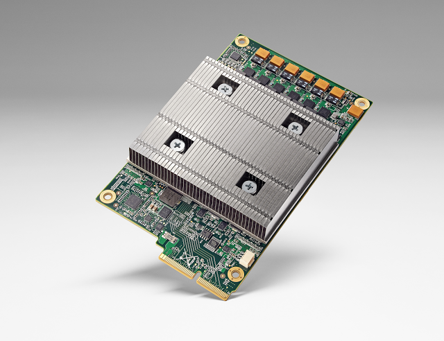
 Last week at the Google I/O conference, it was revealed the search giant has been using its own custom-built ASIC to accelerate the machine learning capabilities that now underlies much of the Google cloud. The microprocessor, known as the Tensor Processing Unit (TPU), was designed by Google engineers to speed up the TensorFlow software that the company uses to drive much of its machine learning functionality. TensorFlow began as a machine learning research project, but later moved into production, and is now deployed in an array of applications, including Google Cloud Speech, Gmail, Google Photos, and Search. According to the company, TPUs have been churning away in their production datacenters for about a year, unbeknownst to its users.
In a blog post penned by Norm Jouppi, a Google engineer said to be deeply involved in the TPU project, he wrote that the accelerator is being utilized in RankBrain to improve search results and in Street View to improve the accuracy and quality of the maps and the navigation. Jouppi also noted that TPUs were used to power AlphaGo, the AI program that vanquished Go champion Lee Sedol in a series of matches in March. The performance bump provided by the purpose-built chip was equivalent to three generations of Moore’s Law, according to Jouppi.
For the vast majority of organizations, designing and building a processor specific to their application set is an unaffordable luxury. Developing a chip typically runs into the tens of millions of dollars, even for relatively simple designs. The advantage of a custom design is that it can provide much better performance and/or energy efficiency compared to a more general-purpose microprocessor. But to recover development costs requires either a very high-value use case or a large-scale deployment where the cost of design, testing and production can be effectively amortized over thousands of chips. Some hyperscale environments may indeed satisfy the latter scenario.

Google CEO Sundar Pichai certainly thinks so. “The scale at which we need to do machine learning is incredible and so we have started building specialized custom hardware,” he explained in his Google I/O conference keynote, later adding that “TPUs deliver an order of magnitude higher performance per watt than all commercially available GPUs and FPGAs.”
Those two statements should give pause to microprocessor vendors like NVIDIA and Intel, both of whom are eyeing machine learning as an opportunity to sell bushels of high-end, high-margin chips into what, by all accounts, is a rapidly growing market. A number of industry analysts are projecting double-digit growth rates for AI-type products and services over the next several years, with an annual market revenue growing to between $5 and $70 billion during this timeframe.
NVIDIA has staked out an early lead in the market with its supercomputing GPUs, and has been busily adding an array of machine learning features into products like the M4 and M40. Their latest and greatest server GPU, the P100, is being pitched primarily as a machine learning accelerator. Intel, with its new “Knights Landing” Xeon Phi and upcoming Altera FPGA-integrated Xeon processors, also has designs on machine learning. Likewise, FPGA-maker Xilinx is taking a look at this market as part of a broader strategy to penetrate the datacenter space.
It’s not clear if Google’s TPUs are being used primarily in machine learning training or execution (inference) systems. The training phase is the most computationally demanding, and the one in which GPUs and FPGAs can be used to greatest effect. A paper on how TensorFlow works says the software can support both capabilities, which suggests that the TPU may have applications in both areas as well. But for what it’s worth, Google has not shown any inclination to dump its existing GPU or CPU servers in its machine learning infrastructure.
In any case, it’s not that these TPU accelerators will upend the commodity processor-based model – at least not yet. But the combination of hyperscale market forces, along with an insatiable desire to maximize price-performance and performance-per-watt, could drive the Googles of the world to bypass conventional chipmakers in the same manner they ditched OEMs when these web giants realized they could get better bang for the buck if they designed their own servers. Designing the chips inside those servers could turn out to be the next logical step.
