March 23, 2018
By: Michael Feldman
Xilinx has unveiled its adaptive compute acceleration platform (ACAP), a new FPGA product category that will form the basis for the company’s push into the datacenter.
According to the press release, ACAP will integrate an FPGA with other programmable components, combining the flexibility of reconfigurable hardware with the software friendliness of more standard digital circuitry. It’s designed to accelerate a range of data-intensive workloads in the datacenter on both servers and edge devices. In particular, Xilinx is aiming ACAP at things like video transcoding, database processing, data compression, search, AI inference, genomics, machine vision, computational storage and network acceleration.
The company is claiming that the first ACAP devices will be 10 to 100 times faster than CPUs for these applications and will have more versatility than either GPUs or ASICs. Some of that versatility is inherent in the reconfigurable nature of FPGAs, whose hardware can be reprogrammed on the fly to switch from say, image searching to genomics analysis, in a matter of minutes. Xilinx says the first iteration of ACAP will be 20 times faster than the company’s latest Virtex VU9P FPGA on inferencing neural networks, one of the key applications the company is aiming at.
"This is a major technology disruption for the industry and our most significant engineering accomplishment since the invention of the FPGA," said Victor Peng, president and CEO of Xilinx. "This revolutionary new architecture is part of a broader strategy that moves the company beyond FPGAs and supporting only hardware developers. The adoption of ACAP products in the datacenter, as well as in our broad markets, will accelerate the pervasive use of adaptive computing, making the intelligent, connected, and adaptable world a reality sooner."
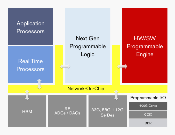
 Image: APAC functional design. Source: Xilinx
ACAP’s key design feature is heterogeneity, implemented as “a new generation of FPGA fabric.” Basically, it’s an integrated device that connects an FPGA with distributed memory and programmable DSP blocks, a multicore SoC (likely ARM-based), and one or more programmable compute engines, all of which are connected through a network-on-chip (NoC) fabric. ACAP also contains programmable I/O and memory controllers, along with an option for integrated high bandwidth memory. The initial product line, codenamed “Everest,” will be implemented using TSMC’s 7nm process technology.
Developers will be able to write software for these devices using traditional programming languages like C/C++, Python and OpenCL. The platform will also be amenable to programming at the register transfer level (RTL) employing standard FPGA tools. By offering a mix of both software and hardware, Xilinx hopes to make the architecture more accessible to application programmers, while also supporting the low-level capabilities that makes the FPGA so malleable.
Xilinx has invested a lot of time and resources into ACAP. To get from the drawing board to Everest has taken four years and occupied more than 1,500 engineers. The FPGA-maker says it has sunk more than a billion dollars into the product line’s development.
This is not Xilinx’s first pass at heterogeneity. Prior to ACAP, Xilinx developed the Zynq product line, which offers FPGAs integrated with ARM processors, DSP blocks, and even GPUs, packaged as an SoC. Zynq products, however, are aimed mainly at the embedded space. ACAP, on the other hand, is focused on computational acceleration, principally in the datacenter, and presumably will pack a lot more computational horsepower onto the die. The biggest Everest products are expected to have around 50 billion transistors. The plan is to tape out the first chips later this year, followed by customer shipments in 2019.
