April 6, 2017
By: Michael Feldman
Although Google’s Tensor Processing Unit (TPU) has been powering the company’s vast empire of deep learning products since 2015, very little was known about the custom-built processor. This week the web giant published a description of the chip and explained why it’s an order of magnitude faster and more energy-efficient than the CPUs and GPUs it replaces.
First a little context. The TPU is a specialized ASIC developed by Google engineers to accelerate inferencing of neural networks, that is, it speeds the production phase of these applications for networks that have already been trained. So, when a user initiates a voice search, asks to translate text, or looks for an image match, that’s when inferencing goes to work. For the training phase, Google, like practically everyone else in the deep learning business, uses GPUs.
The distinction is important because inferencing can do a lot of its processing with 8-bit integer operations, while training is typically performed with 32-bit or 16-bit floating point operations. As Google pointed out in its TPU analysis, multiplying 8-bit integers can use six times less energy than multiplying 16-bit floating point numbers, and for addition, thirteen times less.
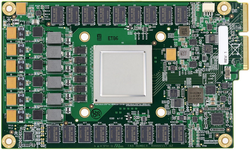
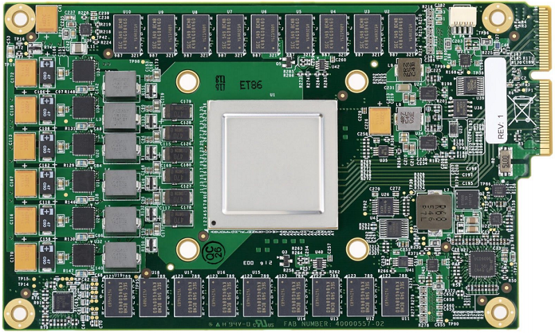 Google TPU Board
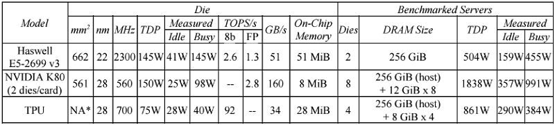
The TPU ASIC takes advantage of this by incorporating an 8-bit matrix multiply unit that can perform 64K multiply accumulate operations in parallel. At peak output, it can deliver of 92 teraops/second. The processor also has 24 MiB of on-chip memory, a relatively large amount for a chip of its size. Memory bandwidth, however, is a rather meagre 34 GB/second. To optimize energy usage, the TPU runs at a leisurely 700 MHz and draws 40 watts of power (75 watts TDP). The ASIC is manufactured on the 28nm process node.
When it comes to computer hardware, energy usage is the prime consideration for Google, since it’s tied directly to total cost of ownership (TCO) in datacenters. And for hyperscale-sized datacenters, energy costs can escalate quickly with hardware that’s too big for its intended task. Or as the authors of the TPU analysis put it: “when buying computers by the thousands, cost-performance trumps performance.”
Another important design consideration for the TPU is response time. Since inferencing is performed in response to user queries, the system needs to deliver the result in near real-time. That meant the TPU designers favored low latency over high throughput. For GPUs, that relationship is reversed, which is one reason why they are so good at the more compute-demanding training phase.
Google’s justification for developing a custom chip for inferencing started building about six years ago when they began incorporating deep learning into more of their core search products. Since these products were being used by millions of people on a daily basis, the computational costs began to look daunting. For example, they determined that if people used a neural net-powered voice search for just three minutes a day, they would have to double the number of Google datacenters, assuming they stuck with conventional hardware.
Since the TPUs are purpose-built for inferencing, it offers much better performance and performance/watt than either Intel CPUs or NVIDIA GPUs. To determine its capabilities, Google compared its TPU against other with 2015-era hardware used for inferencing, specifically Intel’s Haswell Xeon CPU and NVIDIA’s K80 GPU. Tests were performed on six benchmarks of the three most commonly used neural networks: convolutional neural networks (CNN), recurrent neural networks RNN), and multi-layer perceptrons (MLP). The server configurations are illustrated below.
 Source: Google
What they found was that their TPU performed 15 to 30 times faster than the K80 GPU and Haswell CPU across these benchmarks. Performance/watt was even more impressive, with the TPU beating its competition by a factor of 30 to 80. Google projects that if they used the higher-bandwidth GDDR5 memory in the TPU, they could triple the chip’s performance.
Such results are not all that surprising, considering that the K80 GPU is targeted at HPC and neural network training and is not optimized for inferencing. As far as the Xeon CPUs go, they’re not optimized for deep learning codes of any sort, although they are only moderately slower than the K80 for such work.
To some extent, all of this is all old news. NVIDIA’s 2017 crop of Pascal-generation GPU outperform the Kepler-era K80 by a wide margin. On the inferencing side, in particular, NVIDIA now offers the Tesla P4 and P40 GPUs, which, like the TPU, support 8-bit integer operations. Those NVIDIA processors may not be fast enough to catch the customized TPU, but the performance gap between them would probably be narrowed significantly.
In any case, the TPU is not threatening NVIDIA’s deep learning business. The GPU-maker still dominates the training space and is probably going to sell plenty of its P4 and P40 inferencing accelerators to hyperscalers not named Google. The more general threat to NVIDIA on the inferencing side is Intel, which is positioning its Altera FPGAs for this type of work. Microsoft has already signed on to this model, deploying the world’s largest AI cloud using Altera/Intel silicon. Other AI service providers could follow suit.
It’s almost certain that Google is already working on its second-generation TPU. That chip is likely to support higher memory bandwidth, either for GDDR5 or something more exotic. The engineers will also probably fiddle with the logic and block design so they can bump up the clock frequency. Moving to a smaller process node, say 14nm, would make all of this easier. Of course, it’s possible these TPUs are already in production and deployed somewhere in the far reaches of the Google cloud. We’ll find out in two years.