Dec. 12, 2018
By: Michael Feldman
 In what could be Intel’s most significant architectural advance in decades, the chipmaker unveiled a technology that will enable processors and other logic chips to be integrated into 3D packages.
The company says the new technology, named Foveros, will enable it to “continue exponential scaling in computing density by extending transistor density to the third dimension.” It’s no secret that the pace of transistor shrinkage promised by Moore’s Law is slowing, and chipmakers are scrambling for solutions. One of the most talked about solutions is stacking chips into 3D structures. While the transistors themselves won’t get smaller, their density is increased by virtue of going vertical.
Three-dimensional devices are also inherently better at supporting higher performance communication between the stacked components due to the fact that they can be place in such close proximity to one another. This capability has already been taken advantage of in the current crop of 3D memory designs – the Hybrid Memory Cube (HMC) and the High Bandwidth Memory (HBM) – both of which boast significantly higher bandwidth and lower latency than planar memory devices.
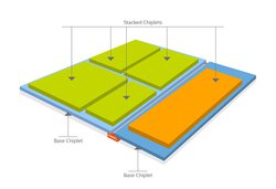
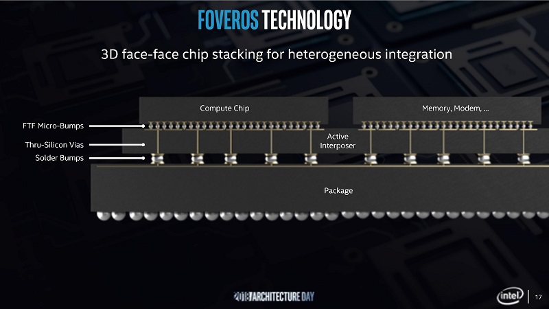
Intel says the Foveros technology can be used to integrate CPUs, GPUs, AI processors, and other specialized logic units in mix and match fashion. Other discrete integrated circuit blocks like analog chips, memory, photonics chips, and FPGAs are also fair game. The chips, or as Intel now refers to them, chiplets, will be stacked on top of an active interposer base die – active in the sense that it contains logic that will perform package management functions. Like its more traditional passive cousin, the active interposer communicates with the dies above it, in this case using thru-silicon vias (TSVs). According to diagrams provided by the company the chiplets will be outfitted with an array of face-to-face (FTF) microbumps to facilitate communication between the stacked components.
One of the big advantages of the technology according to Intel is that the various chiplets integrated into the package can be manufactured using different process nodes to optimize performance and power efficiency. For example, for CPUs you would probably use the most advanced, highest performance node, while for things like I/O and memory controllers, you could get by with less advanced, lower performing nodes. More subtle tradeoffs between cost, power, leakage, and performance can also be exploited by choosing different process technologies. Basically, it enables the package designer to optimize for these criteria at the granularity of the component chiplets, something not possible when building monolithic dies.
It’s worth noting the AMD will also be using a chiplet approach for its Zen 2 Rome CPUs, albeit without the 3D advantages. In this case, the company is manufacturing the Rome’s multiple CPU chiplets using 7nm technology, while the I/O and Infinity Fabric chiplets are manufactured on the less expensive 14nm process node. In fact, the chiplet model also extends to Intel’s existing 2D/2.5D package integration approach based on the company’s Embedded Multi-die Interconnect Bridge (EMIB) technology.
There are plenty of details missing about the underlying technology in Foveros, in particular, what the microbumps and active interposer actually do, and how exactly is chip-to-chip communication performed. Also, how does the technology deal with the heat dissipation challenge of stacked chiplets? The only hint Intel is offering in this regard is that the high performance compute chiplets will be placed on top of the stack, with the lower power chiplets beneath. But that’s not a general solution if you want to construct deep stacks with multiple compute units or other power-demanding dies. As of now, Intel has only demonstrated two-layer devices, with the bottom layer consisting of the active interposer base die.
And then there’s cost. The thing that has restricted 3D memory to specialized applications like high-performance GPUs is that stacked memory is not price-competitive with standard DIMMs on a capacity basis. If Intel is counting on Foveros to pick up where Moore’s Law leaves off, these 3D products not only have to be cost-competitive with planar system-on-chips, but they also have to evolve in such a way that price-performance is continually improved over time as the technology advances.
Obviously, it’s early days for 3D packaging, so we can’t expect everything to be revealed immediately. The first Foverus-based product is scheduled to be released in the second half of 2019. It will combine a 10nm x86 compute die with a 22nm low-power base die, and capped with package-on-package memory. From the looks of it, the package will be targeted at mobile applications.
For the HPC crowd, a more compelling Foverus implementation would be one that integrates x86 Xeon CPUs, AI chips and photonics processors, along with Optane memory and DRAM dies thrown in for good measure. That might turn out to be something close to what we see in the upcoming Aurora supercomputer in 2021. But given Intel’s interest in countering NVIDIA’s and AMD’s high-end ambitions, we may not have to wait that long to see the first 3D packages for HPC.
Images source: Intel Corp.