March 29, 2017
By: Michael Feldman
This week in San Francisco, Intel held its first Manufacturing and Technology Day, an event designed to reassure investors and customers that Moore’s Law is alive and well and delivering the cost and performance benefits it has for the last 50 years. However, to make that claim viable, the chipmaker has recast the law to deal with the realities of a slowdown in transistor shrinkage.
In an editorial published this week by Intel Executive VP Stacy Smith, he writes that “Intel’s ability to advance Moore’s law – to make products less expensive and more capable every year – is our core competitive advantage.” While that may appear to contradict the slowing pace of transistor shrinkage, the company is making the case that it can still deliver the underlying goals of better performance and lower cost.
To start with, Intel is no longer talking about Moore’s Law as doubling transistor density every two years, which itself was a modification of the 1965 version that had it doubling every year. Rather Intel now speaks of improving density with each process node shrink. But those node shrinks are no longer two years apart; they are now three to four years apart.
For example, Intel began manufacturing 14nm chips in 2014, and is not planning to deliver its 10nm silicon until late 2017 at the earliest. Its 7nm chips, which will be produced at the company’s recently announced Arizona facility, are not expected to be available until sometime between 2020 and 2022. As we reported just a couple of weeks ago, the two-year Moore’s Law cadence, which has been in effect since 1975, has slowed significantly.
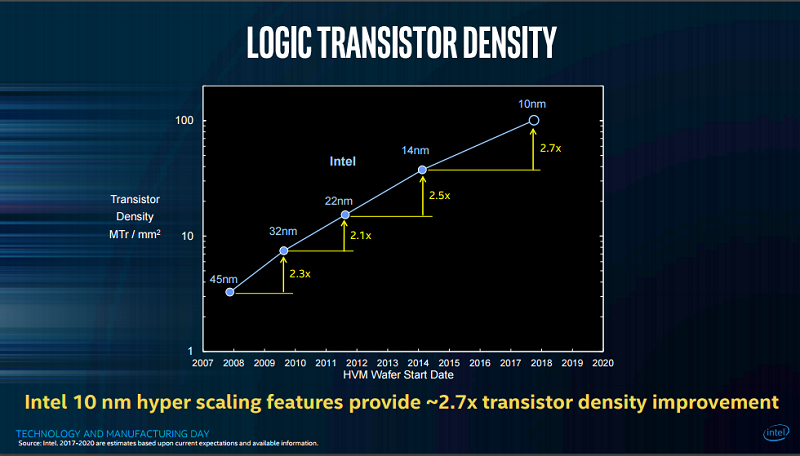
Although Intel did not focus on the extended timeframe between process nodes at this week’s event, the company did admit that “the time between nodes has lengthened.” In fact, one of the graphics in the slide deck presented by Intel Senior Fellow Mark Bohr, explicitly illustrates the longer period between process shrinks.

One thing working in Intel’s favor, is that that transistor density increases per node appears to be better than 2x, even as the timeframe lengthens. The company refers to this process as “hyperscaling.” For example, according to Intel, the jump from 22nm to 14nm increased transistor density by 2.5x, while moving from 14nm to 10nm is expected to improve it by another 2.7x. If the chipmaker can keep that up, the slower pace of process shrinks won’t be as ominous.

Nevertheless, increasing density by 2.7x every three and half years is not as good as doubling it every two years. Intel though, offered a graphic that illustrates their trajectory for increasing transistor density does maintain the 2x/two-year cadence in the long-term. To do that though, you have to ignore the real slowdown that began with the current 14nm node. Looking ahead to 7nm, Intel would have to hyperscale the heck out of its transistors to prevent the curve from flattening further.

One of the other ways Intel is trying to shore up Moore’s Law is by applying manufacturing refinements within a given process node. For example, for the 14nm node, Intel introduced 14+ and 14++ variations that offered better transistor performance and power usage. It intends to do the same with its 10nm technology. The geometries are the same, but the manufacturing tweaks provide better capability before the next process technology is reached. It acts as sort of an intra-node Moore’s Law. And although it doesn’t adhere to Moore’s original intent, it does offer Intel an argument that it can improve transistor performance and cost on a more regular basis.
The other pitch the company made at the event is that it measures its transistor geometries more honestly than its competitors, who are now claiming similar or smaller process nodes than Intel. Here Intel is on firmer ground. There is no standard way to measure transistor size, especially with regard to the latest 3D FinFET technology, and TSMC, Samsung and GlobalFoundries have taken advantage of that to claim smaller geometries than is warranted by their silicon.
TSMC and Samsung will get their 10nm chips to market sooner than Intel, while GlobalFoundries is skipping 10nm and going directly to 7nm in less than two years. But those technologies are not equivalent to Intel’s 10nm and 7nm process nodes, which will be significantly denser than those of its counterparts. In general, Intel appears to be at least one node ahead of its rivals based on actual transistor size and density. The chipmaker has offered a standard way of measuring transistors, but it would be preferable if an independent group like IEEE would come up with a definitive metric for the industry.
In the meantime, Intel is going to continue to beat the drum for Moore’s Law for as long as it can, even if it has to rejigger the law somewhat to deal with its manufacturing challenges. In his editorial, Smith writes that “we have line of sight to 7 and 5nm,” while admitting they don’t exactly know how they will get to that last node. Beyond those technologies, Intel has said little, and the general consensus in the industry is that Moore’s Law will finally succumb to physics at 5nm. At that point, Intel will have to come up some new legislation to keep its investors and customers happy. We can hardly wait.
